![]()
![]()
![]()
![]()
|
|
|
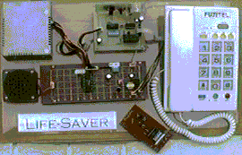
Project Report Life-Saver by April 27, 1997 ContentsContents AcknowledgmentPCB Design and Remote ControllerWe would like to give our most earnest thanks to our project supervisor Dr. Lau and Mr. Poon for their much needed, much appreciated, and invaluable guidance and assistance throughout the project. We would also like to thank Mr. Thomas Lai, Senior Sales Engineer, Angus Electronics Co. Ltd. who sold the core logic IC PT-2262 and PT-2272 in a very small quantity, this initially enable us to commence this part of Life-Saver project. Digital playback/record UnitIt is a pleasure to acknowledge the help of our project supervisor Dr. Lau and our friend Mr. Sheldon and Mr. John Chan whom have given us continued encouragement and every possible form of assistance throughout the entire period of preparation of this section of project. And Mr. Benny Wong who advise us to change from the phase-out 1016/1020 models to current product, the 1416/1420 series. We would also like to acknowledge the people whose participation made the project possible: Mr. Benny Wong Sales Engineer Marubun Hong Kong Ltd. mrbhk@hkisl.net Ms. Bonnie Sales Manager ParcShine Electronics Ltd. parcshin@hkstar.com Mr. David DiGiacomo dd@Adobe.COM Mr. Jaap van Ganswijk ganswijk@xs4all.nl Mr. John Chan Manager ComLogic Technology Co. mlc@glink.net.hk Mr. Sheldon tadedek@flash.net Mr. YK Chan Sales Executive ParcShine Electronics Ltd. parcshin@hkstar.com Project Goals830,000 elderly persons whom age 65 or above living in Hong Kong. Many of them, say thousands are living alone in public rental or private house. Although, the government would increase the total number to 126 teams of professional staffs enabling them to reach out about 12,000 elderly people living alone within the year. There are some unexpected situation may occur for those elder who living alone, such as cold spell in 1995, approximate 30 senior citizen were gone because the temperature suddenly crashed. For example, in the recent cold spell, government has focused attention on the issue of outreaching to elderly persons living alone. In emergency situations like this, the Social Welfare Department mobilizes a large number of professional staff to reach out, but the large number is 63 teams that only enabling them to reach out around 6,000 elder. It quite insufficient compared several thousand elder living alone in Hong Kong. In addition to temperature changing, there are many housing incident such as fire, scald and some severe disease such as cardiac, etc. are grave peril to the elder living alone. Time is life! The faster rescue the more living chance! So, we would like to develop an automatic alarm system, called Life-Saver. Illustration of Life-Saver:
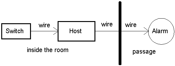
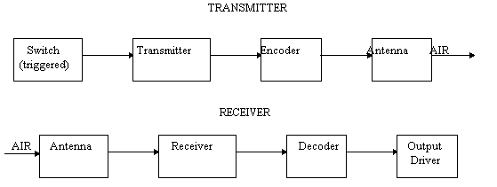
So far as we know, the housing authority currently used a simply alarm
system, a wired system, the brief block diagram as follows,
d:\project\flow chart\fchart00.cfl Compared with our system:
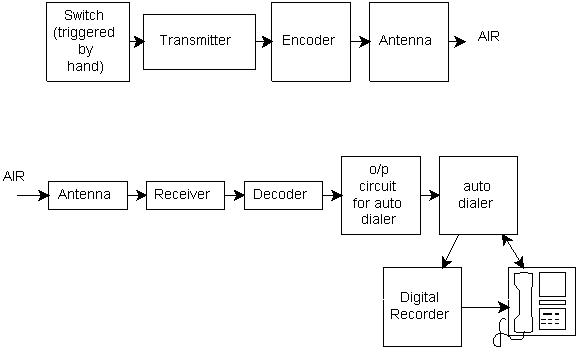
Block diagram of Life-Saver It quite insufficient in emergency used:
The Life-Saver carried out the dramatic function over the traditional one:
Project ObjectivesLife-Saver consists of three major parts, the UHF part, the telecommunication part and the electronics recording part. So, we have the opportunity to practice the knowledge we studied within the two years, such as how to design a ultra high speed PCB described in EDA subject, how to use Op-amp and the filter design described in Network and Circuit Analysis, some special filter - anti-aliasing filter described in embedded system and micro-controller and how to use testing equipment described in Instrumentation. By construct the Life-Saver, we are deeply understood the theory and we studied an ultimate important thing, how to apply the knowledge we got to the actual world. On the other hand, in the modern business society, every produce would face the competitive, how to inexpensive to produce, reliable, safe and easy to use are four major part that affect the market shared of the product. CostBy using non-critical readily available hardware and electronic components. reliabilityBy using solid-state active components and PCB construction techniques, a high degree of reliability will be obtained. SafetyBy using both battery for remote control and an fused power supply, insulated o/p terminals, and a completely plastic enclosure, safe operation will be assured. AppearanceIn order to down the cost, the plastic enclosure, either simply painted or covered with contact paper, will ensure relative attractive but low cost. Ease of useOne-touch triggering with the use of a micro switch on the remote controller, a front panel-mounted LED indicator to acknowledge the signal received to ensure Life-Saver would had a high degree of functionality and be easy to use. Responsibilities
Structure of Life-SaverLife-Saver consists of three major parts:
UHF remote controllerIllustration of UHF Remote Controller
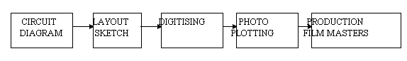
| |||||||||||||||||||||||||||||||||||||||||||||||||||||||||||||||||||||||||||||||||||||||||||||||||||||||||||||||||||||||||||||||||||||||||||||||||||||||||||||||||||||||||||||||||||||||||||||||||||||||||||||||||||||||||||||||||||||||||||||||||||||||||||||||||||||||||||||||||||||||||||||||||||||||||||||||||||||||||||||||||||||||||||||||||||||||||||||||||||||||||||||||||||||||||||||||||||||||||||||||||||||||||||||||||||||||||||||||||||||||||||||||||||||||||||||||||||||||||||||||||||||||||||||||||||||||||||||||||||||||||||||||||||||||||||||||||||||||||||||||||||||||||||||||||||||||||||||||||||||||||||||||||||||||||||||||||||||||||||||||||||||||||||||||||||||||||||||||||||||||||||||||||||||||||||||||||||||||||||||||||||||||||||||||||||||||||||||||||||||||||||||||||||||||||||||||||||||||||||||||||||||||||||||||||||||||||||||||||||||||||||||||||||||||||||||||||||||||||||||||||||||||||||||||||||||||||||||||||||||||||||||||||||||||||||||||||||||||||||||||||||||||||||||||||||||||||||||||||||||||
| Schematic diagram with component detail, interconnections, edge connector specification (refer to Appendix A-3 to A-6). | |
| Component list |
Figure A-7 Component List
| Component code | Value | Description | Footprint Code (PROTEL) |
| POWER SUPPLY | |||
| BRIDGE1 | IN 4001 | Diode | DIODE0.4 |
| R1 | 100 | Resistor 1/4W | AXIAL0.4 |
| Z1 | 12V | Zener | DIODE0.4 |
| C1 | 220UF/16V | E Capacitor | AXIAL0.4 |
| C2 | O.1UF | E Capacitor | RB.2/.4 |
| R2 | 33K | Resistor 1/4W | AXIAL0.4 |
| Q1 | 9013 | Transistor | T0-92A |
| C3 | 1000UF/16V | E Capacitor | RB.2/.4 |
| C4 | 47UF/16V | E Capacitor | RB.2/.4 |
| R3 | 47K | Resistor 1/4W | AXIAL0.4 |
| TRANSMITTOR | |||
| BATTERY | 12V | Battery | AXIAL1.0 |
| SW1 | Dip-switch | RAD0.2 | |
| SW2 | Dip-switch | RAD0.2 | |
| D1 | IN 4148 | Diode | DIODE0.4 |
| D2 | IN 4148 | Diode | DIODE0.4 |
| D3 | IN4148 | Diode | DIODE0.4 |
| D4 | IN 4148 | Diode | DIODE0.4 |
| D5 | IN 4148 | Diode | DIODE0.4 |
| SW3 | DIP-8 | Dip-switch | DIP8 |
| U1 | PT-2262 | IC | DIP18 |
| R4 | 33M | Resistor 1/4W | AXIAL0.4 |
| LED1 | RED LED | LED 3mm | RB.2/.4 |
| R5 | 18K | Resistor 1/4W | AXIAL0.4 |
| L2 | 10UH | Coil | AXIAL0.4 |
| VC1 | 25P | Variable Capacitor | AXIAL0.4 |
| C5 | 3P | Ceramic Capacitor | AXIAL0.4 |
| R6 | 47K | Resistor 1/4W | AXIAL0.4 |
| Q2 | MPSH10 | Transistor | T0-92A |
| R7 | 100 | Resistor 1/4W | AXIAL0.4 |
| RECEIVER-UHF | |||
| L3 | 1 TURN | Coil | AXIAL0.4 |
| VC2 | 5P | Variable Capacitor | AXIAL0.4 |
| C6 | 5P | Ceramic Capacitor | AXIAL0.4 |
| C10 | 100P | Ceramic Capacitor | AXIAL0.4 |
| R10 | 270 | Resistor 1/4W | AXIAL0.4 |
| R12 | 18K | Resistor 1/4W | AXIAL0.4 |
| C7 | 3P | Ceramic Capacitor | AXIAL0.4 |
| Q3 | MPSH10 | Transistor | T0-92A |
| R11 | 33K | Resistor 1/4W | AXIAL0.4 |
| C9 | 100n | Ceramic Capacitor | AXIAL0.4 |
| L4 | 8Turns | Coil | AXIAL0.4 |
| R8 | 2.7K | Resistor 1/4W | AXIAL0.4 |
| C8 | 330n | Ceramic Capacitor | AXIAL0.4 |
| R9 | 5.6K | Resistor 1/4W | AXIAL0.4 |
| R7 | 100 | Resistor 1/4W | AXIAL0.4 |
| R8 | 2.7K | Resistor 1/4W | AXIAL0.4 |
| R9 | 5.6K | Resistor 1/4W | AXIAL0.4 |
| R13 | 18K | Resistor 1/4W | AXIAL0.4 |
| C11 | 330n | Ceramic Capacitor | AXIAL0.4 |
| R14 | 6.8K | Resistor 1/4W | AXIAL0.4 |
| C12 | 1UF/16V | E Capacitor | RB.2/.4 |
| R15 | 120K | Resistor 1/4W | AXIAL0.4 |
| Z2 | 12V | Zener | DIODE0.4 |
| Z3 | 12V | Zener | DIODE0.4 |
| U2 | MC4558 | IC | DIP8 |
| R16 | 6.2M | Resistor 1/4W | AXIAL0.4 |
| C13 | 2P | Ceramic Capacitor | AXIAL0.4 |
| R17 | 120K | Resistor 1/4W | AXIAL0.4 |
| RECEIVER-DECODER | |||
| SW4 | DIP-8 | Dip-switch | DIP8 |
| U3 | PT-2272 | IC | DIP18 |
| R18 | 470K | Resistor 1/4W | AXIAL0.4 |
| R19 | 20K | Resistor 1/4W | AXIAL0.4 |
| D6 | IN 4148 | Diode | DIODE0.4 |
| U4 | MC14013 | IC | DIP14 |
| R20 | 47K | Resistor 1/4W | AXIAL0.4 |
| Q4 | 9013 | Transistor | T0-92A |
| LED2 | RED LED | LED 5mm | RB.2/.4 |
| R21 | 4.7K | Resistor 1/4W | AXIAL0.4 |
| R22 | 4.7K | Resistor 1/4W | AXIAL0.4 |
| RELAY1 | 12V | Relay | SIP8 |
| CON1 | 2-PIN | Socket | SIP2 |
| D7 | IN 4148 | Diode | DIODE0.4 |
| RELAY2 | 12V | Relay | SIP8 |
| D8 | IN 4148 | Diode | DIODE0.4 |
| Q5 | 9013 | Transistor | T0-92A |
| C14 | 47UF/16V | E Capacitor | AXIAL0.4 |
| mechanical specifications such as board size and shape, mounting holes, identification of restricted areas with respect to component height, edge connector | |
| PCB specifications, using single- and double-sided. |
In the photo plotter, the input data are converted back to graphics by photographic (Refer to Appendix A-7 to A-9).
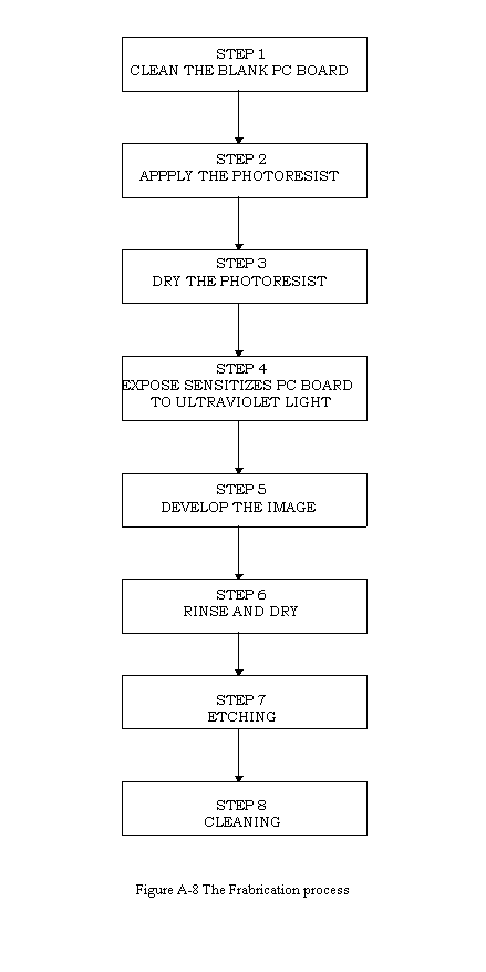
Step 1
Clean the blank PCB. The first step is probably the most important.
Step 2
Apply the Photoresist. While liquid photoresist can be applied by spraying, dipping, speed whirling, and roller coating, these methods are used primarily for mass-production in industry.
When the liquid photoresist is first applied, it really is not yet a resist, but a sensitizer. To take on the properties of a resist that will protect copper underneath, it must be dried and exposed to ultraviolet light.
Step 3
Dry the Photoresist and leave the board in a dark cabinet overnight to let it dry.
Step 4
Expose the Sensitized PCB to Ultraviolet Light. If the board were now placed under an ultraviolet light, the entire sensitized surface would turn to a resist, and no copper could be etched away.
Using an ultra-violet black light, set the printing frame so that it is directly facing the light, approximately 1 foot away. Be sure the surface is exposed to ultraviolet light and that the lamp holder does not cast shadows. Expose for a minimum of 2 minutes. When the exposure is complete, remote the PCB from the frame. The sensitized areas exposed to ultra-violet light are now hard and have formed into a resist.
Step 5
Develop the Image (Pattern). The purpose of the developing step is to remove the unwanted remaining sensitized material (where there was no ultraviolet exposure) and bring out the latent image of the traces and pads. While still under safe-light condition, place the board in a tray filled to a depth of ½ inch with developer. Cover the tray to avoid breathing harmful fumes, and rock the tray gently for about 20 minutes. Then, remove the board and let it drain. At this time return to normal lighting conditions. An image of the traces and pads should now be standing out in clear relief from the surrounding copper.
Steps 6
Rinse and Dry. Under cool, slow running water, rinse the board for 2 t0 3 minutes. Do not let the water hit the board directly, since it could smear the resist pattern.
Step 7
Of all the processes involved in making a PCB, the etching procedure is probably the easiest. Fill the etching container with acid to a depth that will cover the submerged PCB. Ideally, the board should be standing on edge. But if it must lie horizontally, be sure the copper side is facing up. Don't plunge the board into the acid; place it in the container.
Step 8
Using water to cleaning the Acid.
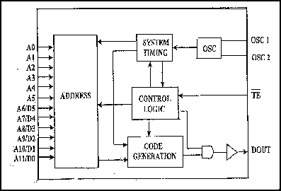
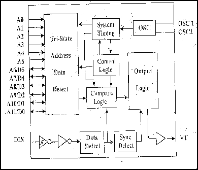
PT2262 is a remote control encoder paired with PT2272 CMOS technology. It encodes data and address pins into a serial coded waveform suitable for RF or IR modulation. PT 2262 has a maximum of 12 bits of tri-state address pins providing up to 531,441 address codes; thereby drastically reducing any code collision and unauthorized code scanning possibilities.
PT2262 encode the code address and data set at A0 ~ A5 and A6/D5 ~ A11/D0 into a special waveform and output is to the DOUT when TE is pulled to "0" (low state). This waveform is fed to either the RF modulator or the IR transmitter for transmission. The transmitted radio frequency or infrared ray is received by the RF demodulator or IR receiver and reshaped to the special waveform. PT 2272 is then used to decode the waveform and set the corresponding output pin(s). Thus completing a remote control encoding and deciding function.
The build-in oscillator circuitry of PT 2262 allows a precision oscillator to be constructed by connecting an external resister between OSC1 and OSC2 pins. For PT 2272 to decode correctly the received waveform, the oscillator frequency of PT 2272 must be 2.5 ~ 8 times that of transmitting PT 2262.
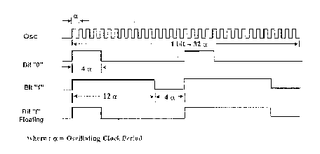
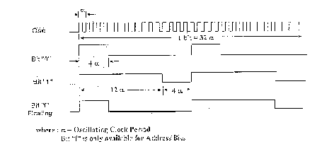
An address/data bit can be designated as bit "0", "1" , or "f" if it is in low, high or floating state respectively . One bit waveform consists of 2 pulse cycle has 16 oscillating time periods. For further details, refer to diagram below:
| PIN NAME | I/O | DESCRIPTION | PIN No. |
| A0 ~ A5 | I | Code address pin Nos. 0 ~5.
These six tri-state pins are detected by PT 2272 to determine the encoded waveform bit 0 ~ bit 5. Each pin can be set to "0", "1" or "f"(floating). |
1 ~ 6 |
| A6/D5 ~ A11/D0 | I | Code address pin Nos. 6 ~ 11/data pin Nos.
5 ~ 0.
These six tri-state pins are detected by PT 2262 to determine the encoded waveform bit 6 ~ bit 11. When these pins are used as address pins, they can be set to "0", "1" or "f"(floating). When these pins are used as data PINS, THEY CAN BE SET ONLY TO "0" OR "1". |
7 ~ 8
12 ~ 15 |
| TE | I | Transmission enable.
Active low signal. PT 2262 outputs the encoded waveform to DOUT when this pin is pulled to low. |
16 |
| OSC1 | I | Oscillator pin No. 1.
A resistor connected between OSC1 and OSC2 determine the fundamental frequency of PT 2272. |
17 |
| OSC2 | O | Oscillator pin No. 2.
A resistor connected between OSC1 and OSC2 determine the fundamental frequency of PT 2272. |
18 |
| DOUT | O | Data output pin.
The encoded waveform is serially outputted to this pin. When PT 2262 is not transmitting, DOUT outputs low(Vss) voltage. |
19 |
| Vcc | Positive power supply | 20 | |
| Vss | Negative power supply | 9 |
PT 2272 is a remote control decoder paired with PT 2262 utilizing CMOS technology. It has a maximum of 12 bits of tri-state address pins providing up to 531,441 address codes; thereby drastically reducing any code collision and unauthorized code scanning possibilities. PT 2272 is available in several options to suit every application needs: variable number of data output pins, latch or momentary output type.
PT 2272 decodes the waveform received and fed into the DIN pin. The waveform is decoded into code word that contains the address, data and sync bits. The decoded address bits are compared with the address set at the address input pins. If both addresses match for 2 consecutive code words, PT 2272 drives:
The build-in oscillator circuitry of PT 22272 allows a Precision oscillator to be constructed with only an external resistor. For the PT 2272 to decode correctly the waveform that was received, the oscillator frequency of PT 2272 must be 2.5 ~ 8 times that of the transmitting PT 2262.
An address/data bit can be designed as bit "0", "1" or "f" if it is in low, high or floating state respectively. One bit waveform consists of 2 pulse cycles. Each pulse has 16 oscillating time periods. For further details, refer to the diagram below:
| PIN NAME | I/O | DESCRIPTION | PIN No. |
| A0 ~ A5 | I | Code address pin Nos. 0 ~5.
These six tri-state pins are detected by PT 2272 to determine the encoded waveform bit 0 ~ bit 5. Each pin can be set to "0", "1" or "f"(floating). |
1 ~ 6 |
| A6/D5 ~ A11/D0 | I/O | Code address pin Nos. 6 ~ 11/data pin Nos.
5 ~ 0.
These six pins are use as higher address input bits or data output pins depending on the version(type) of PT 2272 used. When used as address inputs, these pins are tri-state input pins and each pin can be set to "0", "1" or "f". When used as output pins, these pins are driven to Vcc if
|
7 ~ 8
12 ~ 15 |
| DIN | I | Data Input pin.
The encoded waveform received is serially fed to PT 2272 at this pin. |
16 |
| OSC1 | I | Oscillator pin No. 1.
A resistor connected between OSC1 and OSC2 determine the fundamental frequency of PT 2272. |
17 |
| OSC2 | O | Oscillator pin No. 2.
A resistor connected between OSC1 and OSC2 determine the fundamental frequency of PT 2272. |
18 |
| VT | O | Valid transmission.
Active high signal. VT in high state signifies that PT 2272 receives valid transmission waveform. |
19 |
| Vcc | Positive power supply | 20 | |
| Vss | Negative power supply | 9 |
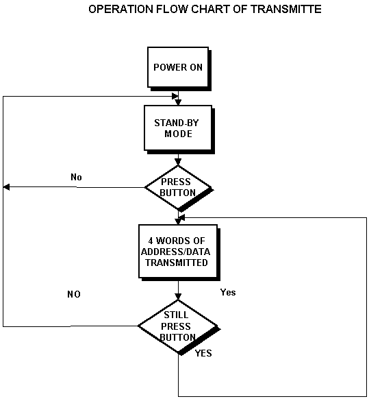
By used the PT 2262, our transmitter circuit is very simple.
For our circuit need a CALL and a RESET button, so we connect two switch connected with A11, A10 and VT , as TE is a active low signal, so we used a diode to make sure a low signal is input.
When we press the CALL button, it will give a signal to A10 and TE. After
encode and mixed with OSC signal. An encoded signal will pass to MSP10(a NPN
type High frequency transistor) and LC circuit which given a high frequency for
transmission.
f = 1/2LC = 1/(6.28*10mH*3.87nF) = 411.25MHz.
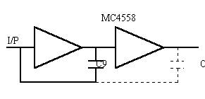
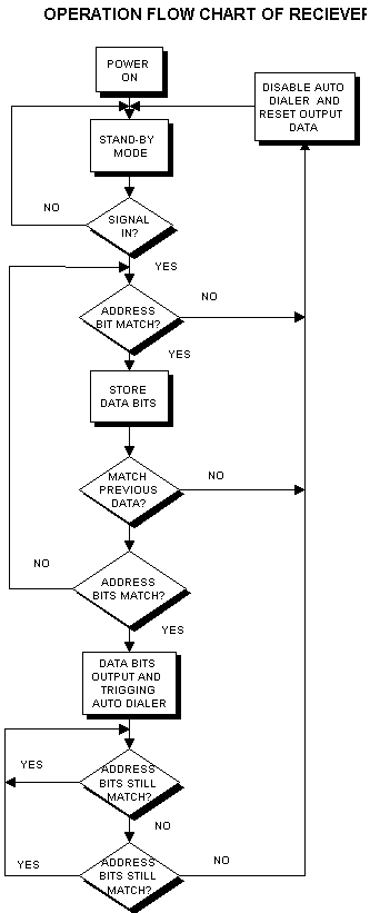
At the first stage of our receiver, we used a turned LC circuit to catch the transmission signal. And pass the MSP10 as a RF amplifier. Then pass a bandpass -active filter which is usedMC4558(a two stage OAMP).
The center frequency f0 = 1/2RC Hz = 26.5 Hz.
At the center frequency the feedback loop passes no current and no attenuation occurs.
Then the second stage of MC4558 is used to amplified the input signal to PT 2272 DIN pin. After decode and PT 2272 will provided a signal to 4013 (a flip flop) which consider by the input signal. If we press the CALL ,button of the transmitter, then the PT 2272 will provide a output from A11 to pin D of 4013 and used 90132 to drive a relay circuit to trigger the auto dialer and digital recorder.
See appendix A-0
| specification | transmitter | receiver |
| Operation Voltage | +12V | +12V |
| Standby Current | 0.3A | 6.3mA |
| Transmitting/Receiving Current | 5.3mA | 23.5mA |
| Transmitting/Receiving Time | 0.5s | 0.5s |
| Operating Temperature | 0C to 70C | 0C to 70C |
| OSC Frequency | 10kHz | 72kHz |
| Transmitting/Receiving Frequency | 411MHz | 411Mhz |
| Carrier Media | Frequency modulation | Frequency modulation |
| Location | Part No. / Value | Description | Unit Price (in HKD) |
| BATTERY | 12V | Battery | $15.00 |
| C1 | 220UF 16V | Ceramic Capacitor | $0.23 |
| C10 | 100P | Ceramic Capacitor | $0.10 |
| C11 | 330n | Ceramic Capacitor | $0.10 |
| C12 | 1UF 16V | E Capacitor | $0.23 |
| C2 | 0.1UF | Ceramic Capacitor | $0.10 |
| C3 | 1000UF 16V | E Capacitor | $0.38 |
| C4 | 47UF 16V | E Capacitor | $0.23 |
| C5 | 5P | Ceramic Capacitor | $0.10 |
| C6 | 5P | Ceramic Capacitor | $0.10 |
| C7 | 3P | Ceramic Capacitor | $0.10 |
| C8 | 330n | Ceramic Capacitor | $0.10 |
| C9 | 100n | Ceramic Capacitor | $0.10 |
| COM1 | 10PIN | Socket | $0.15 |
| D1 | IN 4148 | Diode | $0.12 |
| D2 | IN 4148 | Diode | $0.12 |
| D3 | IN 4148 | Diode | $0.12 |
| D4 | IN4148 | Diode | $0.12 |
| D6 | IN 4148 | Diode | $0.12 |
| D7 | IN 4148 | Diode | $0.12 |
| L2 | 10UH | Coil | $0.12 |
| L3 | 1 Turn | Coil | $0.20 |
| L4 | 8 Turns | Coil | $0.25 |
| LED1 | RED LED | LED | $0.12 |
| LED2 | RED LED | LED | $0.12 |
| Q1 | 9013 | Transistor | $0.16 |
| Q2 | MPSH10 | Transistor | $0.30 |
| Q3 | MPSH10 | Transistor | $0.30 |
| Q4 | 9013 | Transistor | $0.16 |
| R1 | 100 | Resistor 1/4W | $0.03 |
| R10 | 270 | Resistor 1/4W | $0.03 |
| R11 | 33K | Resistor 1/4W | $0.03 |
| R12 | 18K | Resistor 1/4W | $0.03 |
| R13 | 18K | Resistor 1/4W | $0.03 |
| R14 | 6.8K | Resistor 1/4W | $0.03 |
| R15 | 120K | Resistor 1/4W | $0.03 |
| R16 | 6.2M | Resistor 1/4W | $0.03 |
| R17 | 120K | Resistor 1/4W | $0.03 |
| R18 | 470K | Resistor 1/4W | $0.03 |
| R19 | 20K | Resistor 1/4W | $0.03 |
| R2 | 33K | Resistor 1/4W | $0.03 |
| R20 | 47K | Resistor 1/4W | $0.03 |
| R21 | 4.7K | Resistor 1/4W | $0.03 |
| R22 | 470 | Resistor 1/4W | $0.03 |
| R3 | 47K | Resistor 1/4W | $0.03 |
| R5 | 18K | Resistor 1/4W | $0.03 |
| R6 | 47K | Resistor 1/4W | $0.03 |
| R7 | 100 | Resistor 1/4W | $0.03 |
| R8 | 2.7K | Resistor 1/4W | $0.03 |
| R9 | 5.6K | Resistor 1/4W | $0.03 |
| RELAY1 | 12V | **Relay | $0.00 |
| SW1 | Push Bottom | $0.20 | |
| SW1 | Push Bottom | $0.20 | |
| SW3 | SW DIP-8 | **Dip switch | $0.00 |
| SW4 | SW DIP-8 | **Dip switch | $0.00 |
| U1 | PT-2262 | IC | $2.80 |
| U2 | MC4558 | IC | $0.83 |
| U3 | PT-2272 | IC | $2.80 |
| U4 | MC14013 | IC | $0.60 |
| VC1 | 25P | Veriable Capacitor | $0.10 |
| VC2 | 5P | Ceramic Capacitor | $0.10 |
| Z1 | 12V 1/4W | Zener | $0.12 |
| Z2 | 12V 1/4W | Zener | $0.12 |
| Z3 | 12V 1/4W | Zener | $0.12 |
| PCB1 | PCB | 2 Layers PCB | $1.50 |
| PCB2 | PCB | 2 Layers PCB | $1.50 |
| PCB3 | PCB | 2 Layers PCB | $1.50 |
| RELAY2 | 12V | **Relay | $0.00 |
| Q5 | 9013 | Transistor | $0.16 |
| D8 | IN 4148 | Diode | $0.16 |
| C14 | 470UF 16V | E Capacitor | $0.23 |
| Total Amount: | $33.14 | ||
| **Will not use when mass produced. | |||
| It should be noted that the price listed above for large volume only. | |||
The auto dialer circuits consists of two ICs.
1. TP5700A
Telephone Speech Circuit
| The TP5700A is a linear bipolar device which includes all the functions required to build the speech circuit of a telephone, Figure C-1, C-2 |
- It can be directly interfacing to a low voltage DTMF generator, Figure C-3 is shown.
- It can reduce the number of components required to build a pulse dialing telephone,
as shown in Figure C-4.
| The low voltage design enables the circuit to work over a wide range of operating conditions, including long loops, extension telephones and subscriber carrier applications. | |
| Operating power is derived from the telephone line. |
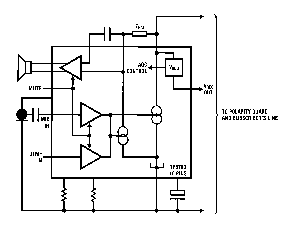
Figure C-2 Simplified Block Diagram
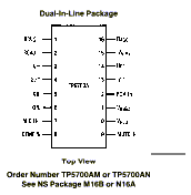
Figure C-2 Connection Diagram
Features :
| 5mA~20mA loop operation | |
| Voltage swing down to 1.0V | |
| Electret microphone amplifier | |
| Receive amplifier with push-pull outputs | |
| Automatic gain compensation for loop length | |
| Sidetone impedance independent of input impedance | |
| DTMF interface with muting | |
| Voltage regulator outputs for DTMF generator etc. | |
| Works in parallel with a standard phone on 20 mA loop | |
| Available in small outline surface mount package |
2. MC145416
Tone/Pulse Dialer with
10 Number Memory
Plus 3 Emergency Numbers
Low-Power, Silicon-Gate CMOS
| The MC145416 is a member of the Motorola HCMOS dialer family, Figure C-5 | |
| 3 X 18 dedicated memories | |
| Signal output inhibited during memory storage | |
| Note pad programming and convenient operation sequence by 5 X 4 keyboard interface |
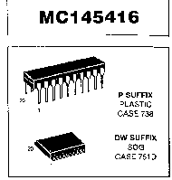
Figure C-5 MC145416 Pin assignment Diagram
Features :
| Stand-Alone Pulse, DTMF, or Mixed Dialing | |
| Pacifier Tone Output at Pulse Dialing | |
| Dialing Mode, Pin Selectable, and Changed by Keyboard Entry | |
| Uses Low Cost 3.57954MHz TV Color Burst Crystal | |
| PABX Pause Storage | |
| Cascaded Memory Redial and Dialing Mode Storage | |
| Dialing Mode Indication Output for Driving an LED | |
| 10 X 8 Digit Memory Storage Inclusive of LNR plus 3 X 8 Digit Dedicated Memory | |
| 40/60 Make Break Ratio, 33/67 in Metal Option # | |
| Flash Function for Transfer Call in a PABXE Environment |
1. Actual Components
Motorola manufactures a series of combination dialing circuits; the MC145412,
MC145413, MC145416, and MC145512. Figure C-6 is a block diagram for the
MC145412/12/16/512 family. Each dialer interfaces directly with either 3 X 4 or
4 X 4 or 5 X 4 keypads. A single input pin will select between DTMF, 10 pps, or
20 pps dialing. An internal memory can hold up to 10 complete telephone numbers,
each up to 18 digits long - this includes last number redial. Finally, the
dialers operate on line power as low as 1.7 volts.
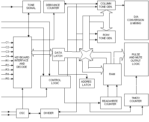
Figure C-6. Combined Dialer Block Diagrm. (Courtesy Motorola, Inc.)
Figure C-7 demonstrates an actual application of the MC145416. A
standard 5 X 4 keypad is used to select desired digits. Keypad signals are
connected to row and column inputs. A ground condition at the off-hook input
will enable the dialer. While on-hook, numbers may be entered into memory
without dialing signals being generated. A 3.58 MHz color burst crystal provides
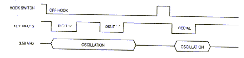
a stable time base for operation. Figure C-8 is shown a timing diagram.
Figure C-7. Combined Dialer Application
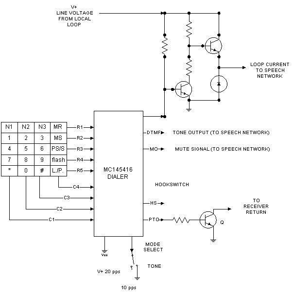
Figure C-8. Timing diagram
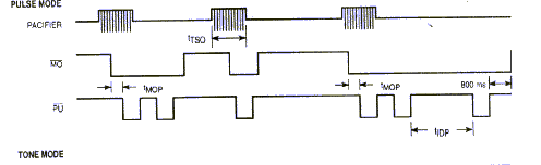
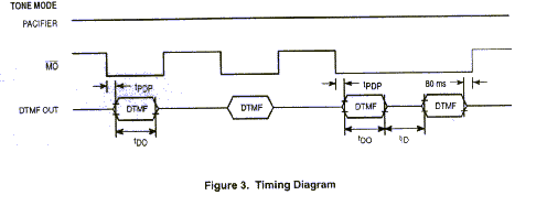
Dialing mode select can be logic high for 20 pps, open for 10 pps, or ground for DTMF signaling. DTMF tones are output to the DTMF OUT pin when the dialer is in the tone mode, and the pulse output (OPL) will be at high-impedance. In pulse dialing mode, the DTMF OUT pin is at high-impedance while pulses are delivered to the OPL pin. Mute is connected directly to the speech network. It will be logic low during pulsing or tone output, otherwise it will be logic high.
Make/break ratios are not field adjustable in the MC145416. Devices are mask programmed at the factory. Both the MC145416. Devices are mask programmed at the factory. Both the MC145412/13/16 offer a typical make/break ratio of 40/60. The MC145512 has a make/break ratio of 32/68.
Memory access and last number redial are accomplished easily by the integrated dialing circuits. For last number redial, the "*" and "0" buttons must be pressed. To retrieve a stored number, "*" and the corresponding number (1 through 9) must be pressed. A complete explanation of dialing key sequences is available in the MC145416 datasheet, Appendix C.
2. A complete integrated auto dialer circuit
Integrated circuit tone/pulse dialing and speech circuit functions can be combined to form a complete, solid-state telephone which can provide such features as tone or pulse dialing with memory and redial, and an active speech network free of bulky transformers or coils. Figure C-9 is the complete schematic for a auto dialer circuit.
Figure C-9 A complete auto dialer circuit, refer to appendix C.
See appendix C-0
| Operating power | derived from the telephone line |
| Core logic | MC145416 / National TP5700A |
| DC supply voltage | -0.5V to 8.0V |
| Operating temperature, TA | -30 oC to +70 oC |
| Power dissipation | 1W |
| 10 number memory | |
| 3 emergency numbers | |
| Loop operation | 5mA-20mA |
| Location | Part No. / Value | Description | Unit Price (in HKD) |
| C1 | 0.01uF | Ceramic Capacitor | $0.10 |
| C2 | 100uF | Ceramic Capacitor | $0.10 |
| C3 | 10nF | Ceramic Capacitor | $0.10 |
| C4 | 47nF | Ceramic Capacitor | $0.10 |
| C5 | 0.22uF | Ceramic Capacitor | $0.10 |
| C6 | 1nF | Ceramic Capacitor | $0.10 |
| C7 | 0.1uF | Ceramic Capacitor | $0.10 |
| C8 | 4.7uF | Ceramic Capacitor | $0.10 |
| R1 | 10 | Resistor 1/4W | $0.03 |
| R2 | 620 | Resistor 1/4W | $0.03 |
| R3 | 470 | Resistor 1/4W | $0.03 |
| R4 | 68 | Resistor 1/4W | $0.03 |
| R5 | 1K | Resistor 1/4W | $0.03 |
| R6 | 1.5K | Resistor 1/4W | $0.03 |
| D1 | IN4001 | Diodes | $0.03 |
| D2 | IN4001 | Diodes | $0.03 |
| D3 | IN4001 | Diodes | $0.03 |
| D4 | IN4001 | Diodes | $0.03 |
| ZD | 18V | Zener Diodes | $0.03 |
| OSC | 3.579545 | Oscillator | $0.03 |
| U1 | TP5700A | IC | $9.00 |
| U2 | MC145416 | IC | $27.30 |
| Keypad | 4X5 | Keypad | $16.00 |
| SP1 | Speaker (8W) | Primd DH31 or Similar | $2.00 |
| MC1 | Microphone | Primd EM80-PM12 or Similar | $0.80 |
| Soc1 | input | 4 pins socket | $5.00 |
| Soc2 | output | 4 pins socket | $5.00 |
| PCB | PCB | 2 Layers PCB | $1.50 |
| Total Amount: | $71.00 | ||
3. Sidetone Circuit and Adjustment
That portion of the talkers voice which is fed back to his/her receiver.
For the hybrid used in the central office exchange, the balancing network is adjusted so that no transmit signal appears at the receive terminals and no receive signal appears at the transmit terminals. However, for the induction coil arrangement in the auto dialer set, the balancing network is internationally unbalanced slightly so that a small amount of the transmitted signal is also fed to the receiver of the talking phone. This signal is called the sidetone.
Sidetone is necessary so that the person can hear his/her own voice from the
receiver to determine how loudly to speak. The sidetone must be at the proper
level because too much sidetone will cause the person to speak too softly for
good reception by the called party. Conversely, too little sidetone will cause
the person to speak so loudly that it may sound like a yell at the other end. In
the circuit shown in Figure C-10, the values chosen for two resistance
and a capacitance produce the proper level sidetone for most conditions .
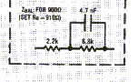
Figure C-10 sidetone circuit
The level of sidetone cancellation may be adjusted by connecting an external balance impedance to SIDETONE (pin 4) and coupling this point to V+. For good sidetone cancellation the balance impedance should be approximately 10 times the subscriber line input impedance. Some typical component values to match a precise 600 ohm termination for test purposes are shown in Figure C-11(refer to appendix C).
The component values used for ZBAL should be selected to provide a clear sidetone sound without excessive "hollowness". The capacitor value and ratio of the two resistors will fix the pole location. To avoid reducing the low voltage performance of the circuit the sum of the two resistors should not exceed 10 KW.
4. DTMF Dialing Using Integrated Circuits
To generate DTMF tones electronically, keypad closures are digitally converted into combinations of low and high frequency sine waves, which are mixed in pairs and amplified, to drive the speech network.
Dialing also may be accomplished by sending dual tones onto the line as discussed for the conventional phone. Integrated circuits have been designed to provide this function. The conventional way of accomplishing this is shown in Figure C-12a. Unlike the conventional way, in which a low-frequency and high-frequency sine wave oscillator feed the speech network, the integrated circuit DTMF generator (Figure C-12b) has a counter and decoder that counts pules from a crystal-controlled oscillator and provides output codes that correspond to the low-frequency tone required and the high-frequency tone required. Each of the two outputs from the counter feed into its own digital-to-analog (D/A) converter. the D/A converter, as the name implies, converts the digital code out of the counter to a sine-wave tone.
Figure C-12. DTMF Generators
4.2 Operational information
Activation of the tone output circuits in the integrated circuit DTMF
generator begins with the caller pressing a key on the keypad. The keypad
contacts may be arranged as shown in Figure C-13a. The top schematic is a
representation of a standard DTMF keypad (like a double-pole single-throw
switch) where a separate set of two contacts give the row and the column of the
key being pushed. An alternative and somewhat less expensive arrangement is
shown in the bottom schematic which is a so-called Class-A or single-pole
single-throw configuration, with only one set of contacts for each row-column
intersection. Some Ics are designed to accept both types; others accept only one
type. In either case, the closed keypad contacts give an indication of the key
being depressed. In some cases, the closed contacts may apply a supply voltage
on the output lines for as long as the key is held down. In other cases, a
ground or the common side of the power supply may be provided. The keypad may be
arranged to provide only a pulse, as is the case for a keypad that is used with
a scanning sequence. The output waveform are shown in Figure C-13b.
Figure C-13. Keypad Contact Types and Output waveform
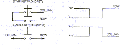
Figure C-13a Figure C-13b
5. Protection Circuit
5.1 Overvoltage Protection
The electronic circuits are protected from high voltage spikes on the line by zener diodes.
Figure C-14 Overvoltage circuits

5.2 Polarity Protection
Polarity reversal is prevented by the rectifier bridge.
Polarity of the normal input voltage is critical for electronic circuits since they won't operate if the polarity is reversed, and they may be damaged. The method commonly used to protect against polarity reversal is the rectifier bridge. The output voltage polarity of a rectifier bridge is always the same regardless of input voltage polarity.
For line voltage of less than 5 volts, the low-voltage rectifier bridge is used. Its forward voltage drop is low because the conducting transistors are at saturation. The transistors are subject to voltage spike damage, however, and are therefore protected by Zener diodes.
6. MC145416
6.1 SWITCHHOOK
6.1.1 On-Hook
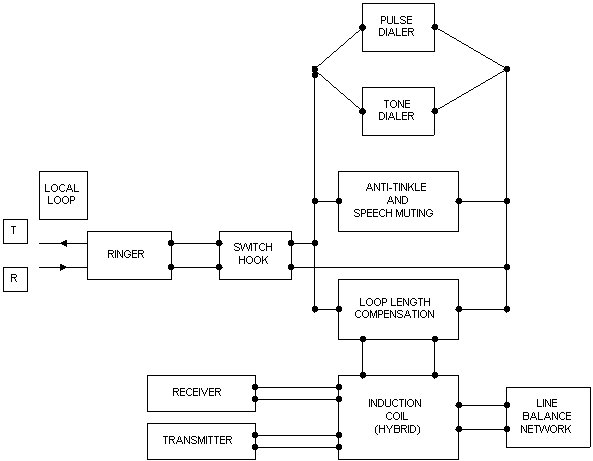
Figure C-15 is a block diagram of a telephone set which shows the major functions. The ringer circuit, which will be discussed later, is always connected across the line so it can signal an incoming call. The remainder of the telephone set is isolated from the line by the open contacts of the switchhook when the handset is on-hook. No dc flows (except possibly a small leakage current) since the ringer has a capacitor that blocks dc flow through it.
Figure C-15 Dialer set Block Diagram
6.1.2 Off-Hook
In the off-hook condition, the closed switch-hook contacts begin a sequence of events in the central office. Initially a relay is energized and a line searcher finds the off-hook line. Then a connection is established, sending a dial tone.
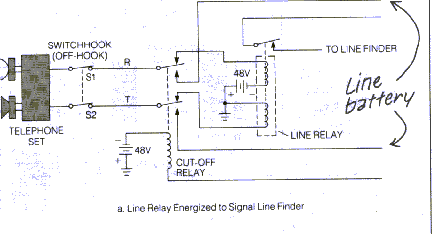
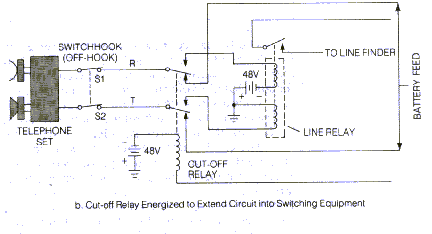
Figure C-16 Line interface relay operation
6.2 Dial interface
The Motorola MC145416 contains a tone amplifier and interface circuit designed to connect dialing signals directly to the loop. Figure C-17 is a diagram of the dial interface. Pin 11 (MS) is a mode select input which switches the mute logic between tone and pulse dialing modes. In this way, the circuitry can provide the appropriate muting signals for tone or pulse dialing. Mode selection must also be connected to the respective dialing circuit.
The mute signal from the dialer is sent to pin 12 (MO). It is this input which supplies the logic control signal the at mutes the receiver. Tone dialing signals can be connected directly to pin 19 (DTO). These signals will be amplified directly by the dial amplifier, AD, and sent along to the local loop.
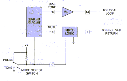
Figure C-17. Dial Interface
Redial function
With the memory function available, it was relatively easy to incorporate a redial function. By pushing only one button, the last number entered will be redialed. This feature is helpful when continually trying to reach a busy number. Initially, the redial feature met with some resistance from the telephone companies because of fears of clogging the network since redialing could be done so rapidly and frequently. also, they were concerned about the maintenance of batteries used to power the electronic circuits in the telephone set. The development of complementary metal-oxide-silicon (CMOS) semiconductor technology, which produces integrated circuits with very low power consumption, has solved the latter problem. The current drain of these circuits is only a few micro-amperes so that it is possible to operate the electronics from the dc power available from the telephone line. However, if a battery of the type commonly used to power calculators or other consumer electronic goods were used to provide only the very small current required by the number memory, the battery would last for several years.
A. Manual Dialing - OFF-HOOK D1 ------------ DN
B. Last Number Redial - OFF-HOOK LNR/PS
When this is the first key depressed after off-hook, excluding Mode Select Switch, it causes the last number entered from the keypad to be dialed out.
ENTERED ......
Mode Select Switch to Pulse Mode, ENTER;
D1 --------- D PS/S D ---------- DN
Pulse input Mode DTMF input
Change with pause
REDIALED ......
ON-HOOK to OFF-HOOK
Mode Select Switch in Pulse Mode, ENTER;
LNR/PS ,Dial out is the same as original entry.
REDIALED ......
ON-HOOK to OFF-HOOK
Mode Select Switch in Tone Mode, ENTER;
LNR/PS ,Dial out changes to"
D1 --------- D D ---------- DN
DTMF input PUSE DTMF input
C) Dialing with auto access pause - OFF-HOOK
ENTERED ......
Mode Switch in either Pulse or Tone Mode
D1 --------- D LNR/PS D ---------- DN
REDIALED ......
ON-HOOK to OFF-HOOK
Mode Select Switch Unchanged, ENTER;
LNR/PS ,Dial out is the same as original entry.
D1 --------- D PAUSE D ---------- DN
D) Dialing with auto access pause and mode change - OFF-HOOK
ENTERED ......
Mode Select Switch in Pulse Mode (10 or 20 pps)
D1 --------- D PS/S D ---------- DN
Pulse Dialing Mode Tone input
Change with pause
ENTERED ......
Mode Switch in Tone mode
D1 --------- D PS/S D ---------- DN
Tone Dialing Pause Tone input
Change with pause
E) Memory storage and recall - OFF-HOOK
REDIALED ......
a) Mode Select Switch in Pulse Mode (10 or 20 pps)
Memory Store Sequence ......
MS D1 ------ D PS/S D ------ DN MS A
Pulse mode Mode Tone mode A = 1-9
Change with pause or N1, N2, N3
ON-HOOK to OFF-HOOK ENTERED ......
Memory Recall Sequence ......
MR A A=1-9 Dial out is: D1 ------ D D ------ DN
Pulse mode Mode Tone mode
Change with pause
b) Mode Select Switch to DTMF
Memory Recall Sequence ......
MR A A=1-9 Dial out is: D1 ------ D D ------ DN
Tone mode Pause Tone mode
REDIALED ......
a) Mode Select Switch in Tone Mode
Memory Store Sequence ......
MS D1 ------ D PS/S D ------ DN MS A
Tone mode Pause Tone mode A = 1-9
Change with pause or N1, N2, N3
ON-HOOK to OFF-HOOK ENTERED ......
Memory Recall Sequence ......
MR A A=1-9 Dial out is: D1 ------ D D ------ DN
Tone mode Pause Tone mode
b) Mode Select Switch in Pulse Mode (10 or 20 pps)
Memory Recall Sequence ......
MR A A=1-9 Dial out is: D1 ------ D D ------ DN
Pulse mode Pause Tone mode
Change with pause
F. Cascaded dialing - OFF-HOOK
a) Numbers stored with the Mode Select Switch set to pulse (10 or 20 pps) can be dialed out as follows:
ENTERED ......
| N1 N2 Both N1 and N2 will dial out as originally stored. |
ENTERED ......
| N1 PS/S N2 N1 will dial out as stored, N2 will convert to DTMF. PTO output will remain active during the dial out of N2. |
ENTERED ......
PS/S N1 N2 Both N1 and N2 will dial out in DTMF, with PTO active.
|
ENTERED ......
| MR A LNR Both MR A and LNR dial out in pulse |
ENTERED ......
LNR MR A Both LNR and MR A dial out in pulse
|
4. The second control key, or number input, has to be entered after completion of the previous dialing.
G. Flash - OFF-HOOK FLH
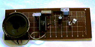 Prototype
We would like to separate this section into two parts:
See Appendix D-1
The detailed PCB layout such as shield screen, bottom layer, top lay, etc. it also consists of different scaling 1:1 and a fit to page printout, easy read the PCB in a relative large size, please see Appendix D-2 page 1 through 13.
Specifications for D:\PROJECT\DIGITA~1\RPPROJEC.PCB
On 6-Apr-1997 at 17:20:17
Size of board 0.301 x 0.375 sq. in
Equivalent 14 pin components 1.520 sq. in/14 pin component
Components on board 28
Layer Route Pads Tracks Fills Arcs Text
![]()
Top Layer Vertical 0 228 0 0 0
Bottom Layer Horizontal 0 255 0 0 0
Top Overlay - 0 170 0 4 0
Multi-Layer - 104 0 0 0 0
![]()
Total 104 653 0 4 0
Layer Pair Vias
![]()
Top Layer - Bottom Layer 17
![]()
Total 17
Hole Size Pads Vias
![]()
28mil (0.7112mm) 5 17
32mil (0.8128mm) 99 0
![]()
Total 104 17
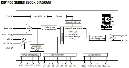
For detailed pins description please refer to appendix D-3. The data sheet shows the detailed description of ISD14xx series and 10xx series chips.
ISD 1416 supports several operational modes as follows:
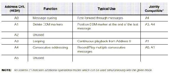
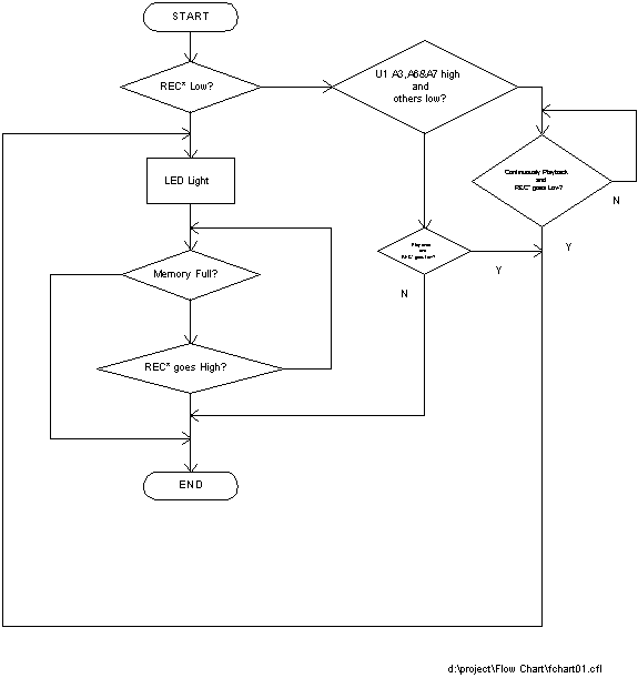
For our special purpose, we would like to choose A3 - Looping mode for message continuously playback. So, the ISD 1416 pin 4 (A3), 9(A6) and 10 (A7) are pulled high after message recorded, it should be noted that A3 and A6 pulled high indicates the chip running in the operational mode and the addressing mode. In order to achieve the such mode, a 3 pins jumper S1 employed that pull the such three pins high while either playback or standby and low while recording.
In order to obviously demonstrate the digital recorder unit, our prototype unit connected an 8W speaker permanent to the sp+ and sp- pins through two 18W resistors (R8, R9) in parallel (impedance matching purpose, (18//18)+8=17W , the rated output impedance be at least 16 W.) and a dip switch that control the PLAYE* pin connected to either ground or Vcc, since the signal triggered by a negative going pulse, not the voltage level, a micro switch would more suitable for the purpose. But we get a four switches dip switch, we prevent the waste of components, using that instead of the micro switch. There are two different mode of playback triggering method we can use, the level trigger and the edge trigger. We chose edge trigger because it easy interfacing so that increasing the connectivity and future expansion of our project, so we connected the PLAYL* always to Vcc. And use the PLAYE* input as the trigger pin. By switching on and then of the dip switch S2-sw3 (simulate a negative going pulse), the automatic playback looping commence until:
According to the purpose we required, there is no need to stop the playback process once it triggered.
All address pins A0 through A7 are pulled low for recording mode. By connecting with a telephone, the Microphone section can be totally eliminated, and then connect the microphone of telephone handset directly to 1416 ANA IN pin (pin 20). Therefore, we can eliminate MC1, C3 - C6, R2 - R5, quite reduce the manufacturing cost. In fact, there are some interfacing circuit may be need to match the handset microphone and the 1416 ANA IN pin input characteristics. For demonstration purpose, we add all of such components to show the demo unit easily. The C4, C5 MC1 are tied together and then connected to MIC and MIC REF pin of 1416 carried out the following purpose:
R5, C6 give the time constant for the release time and an internal 5K resistance and C6 give the time constant of the attack time, by calculation, 5K*4u7=23.5mS, say the gain would pulled-down within 23.5mS when a louder sound attacked. On the other hand, by employed the R5, a 470KW resistor, applied the formula above, we got 470K*4u7=2.209S, say the gain would gradually increase within approximate 2.2 seconds, the release time quite longer than the attack time because sound usually decrease in a slow gradient while the sound sudden increases. They help the AGC dynamically adjusts the gain of the preamplifier to compensate for the wide range of microphone input levels. Allows full range of sound to be recorded with minimum distortion.
In order to prevent unexpected recording taking place when circuit is powered up or Vcc rises faster than REC*. This undesired recording prevents playback of the previously recorded message. A spurious End Of Message (EOM) marker appears at the very beginning of the memory, preventing access to the original message, and nothing is played. To prevent this occurrence, we place C7 between the control pin (REC*) and Vcc. This pulls the control pin voltage up with Vcc as it rises. Once the voltage is HIGH, the pull-up device will keep the pin HIGH until intentionally pulled LOW, preventing the false EOM marker.
An LED (D1) in series with an R7 (1K) resistor (current limitation) connected to RECLED* to indicate that the recording process taking place.
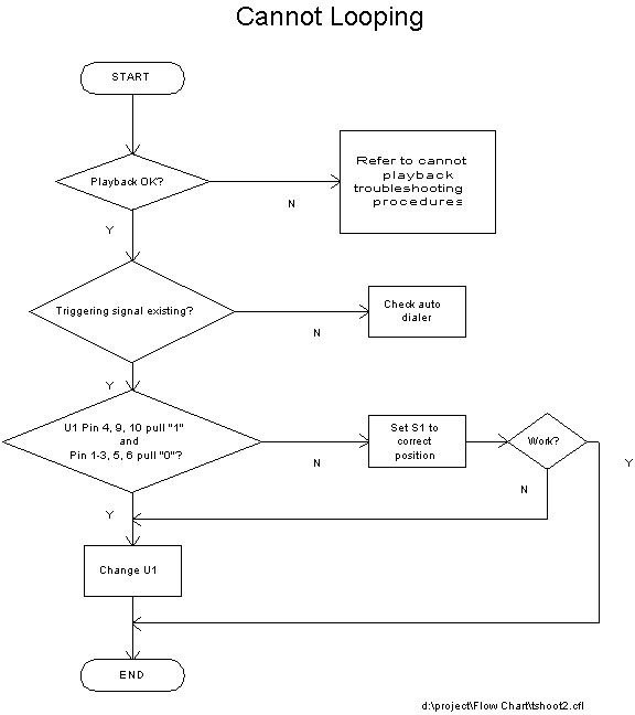
The whole circuit operation please refer to the following flow chart:
Pin assignment of ISD 1416:
The ISD1416 ChipCorder® devices is controlled by a single record signal, REC*, and either of two playback control signals, PLAYE*, and PLAYL*.
ChipCorder® technology provides a means of storing information directly, without conversion to digital, into standard EEPROM memory cells. Utilizing a patented multi-level storage technique, the devices currently store up to eight times the information per memory cell compared to conventional digital solutions.
Since EEPROM cells are non-volatile, 1416 does not require battery backup to preserve the recorded message. Overall power consumption, therefore, is dramatically reduced.
The most different between ChipCorder® technology and traditional AD/DA technology is that enables storage of analog signals directly into memory, eliminating the need for analog-to-digital conversion. This not only minimizes, but also simplifies, the external circuitry required. Furthermore, 1416 also integrated the oscillator, microphone pre-amplifier, AGC, antialiasing filter, smoothing filter and speaker amplifier on-chip, quite reduces the circuit complication.
1416 using "Multi-level" storage that is a high-density storage methodology. Conventional digital storage, for example, stores one "bit" of information per memory cell - a "1" or a "0" (or, in terms of voltage levels, an "on" or an "off"). 1416 improves on this and stores up to 256 distince voltage levels per single cell! So, 1416 is able to store up to 8 times (2 to the power of 8 = 256) more information in the same amount of memory space.
Internal block diagram of 1416/20 series:
S1 |
2-3 |
shorted |
S2 |
sw4 ON |
others OFF |
2. Red LED lights, recording process commencing …
1. set the switch as follows,
S1 |
2-3 |
shorted |
S2 |
sw4 ON |
others OFF |
2. Red LED lights, begin recording message …
It should be noted that since there unit store the message in an advanced technology, there is no need to connect power to retain the message you recorded.
Since the auto dialer would automatically triggered the unit to play your message recorded, should you will not need to do anything once you recorded the desired message.
Should you want to revise the message, do not worry! It is able to re-record up to 100,000 times.
Should you have any question please do not hesitate to contact us.
See appendix D-0
| Operating Voltage | +4.5V to +5.5V |
| Standby Current | 0 |
| Recording/Playback Current | 15mA / 25mA |
| Recording time | 16 seconds |
| Operating Temperature | 0 oC to 70 oC |
| Speaker Output Impedance | 16 W |
| Sampling Rate | 8KHz |
| Message Backup Current | 0mA for 100 years message retention |
| Record Cycle | 100,000 times |
| Core Logic | ParcShine™ ISD 1416P |
| Location | Part No. / Value | Description | Unit Price (in HKD) | |
| C7 | .001UF | Ceramic Capacitor | $0.10 | |
| C3 | 0.1UF | Ceramic Capacitor | $0.10 | |
| C5 | 0.01UF | Ceramic Capacitor | $0.10 | |
| C4 | 0.01UF | Ceramic Capacitor | $0.10 | |
| C2 | 0.1UF | Ceramic Capacitor | $0.10 | |
| R7 | 1K | Resistor 1/4W | $0.03 | |
| R1 | 1K | Resistor 1/4W | $0.03 | |
| C6 | 4.7UF | E Capacitor | $0.23 | |
| R6 | 5K | Resistor 1/4W | $0.03 | |
| VR1 | 5K | *Variable Resistor | $0.03 | |
| R2 | 5K1 | Resistor 1/4W | $0.03 | |
| R4 | 10K | Resistor 1/4W | $0.03 | |
| R3 | 10K | Resistor 1/4W | $0.03 | |
| C9 | 10UF 16V | E Capacitor | $0.23 | |
| C8 | 10UF 16V | E Capacitor | $0.23 | |
| R8 | 18W | Resistor 1/4W | $0.03 | |
| R9 | 18W | Resistor 1/4W | $0.03 | |
| RP2 | 47K | Resistor 1/4W | $0.03 | |
| RP1 | 47K | Resistor 1/4W | $0.03 | |
| C1 | 220UF 16V | E Capacitor | $0.23 | |
| R5 | 470K | Resistor 1/4W | $0.03 | |
| U1 | ISD 1416 | IC | $27.40 | |
| MC1 | MICROPHONE | Capacity Microphone | $0.80 | |
| S1 | NOR/LOOP | Jumper | $0.20 | |
| D1 | REC LED | LED | $0.12 | |
| S3 | SP/HANDSET MIC | Jumper | $0.20 | |
| SP1 | SPEAKER (8W) | **Speaker for indication only | $0.00 | |
| S2 | SW DIP-4 | Dip switch | $1.50 | |
| PCB | PCB | 2 Layers PCB | $1.50 | |
| Total Amount: | $33.50 | |||
| Remarks: | ||||
| *Will change to resistor when mass produced. | ||||
| **For display only. | ||||
| It should be noted that the price listed above for large volume only. | ||||
D:\project\report writing\Digital Recoder BOM.xls
Initially, we received the original idea for construct the digital recorder by using ISD 1016/1020 from the friend of Internet. After visit the Information Storage Device Corporation's wet site, we got the data sheet of 1016/1020 and 2590 chips and found also that there are two local distributors existed. Since there is few time for us to construct digital recorder, we design the circuit while trying to find the 1016 chip. 2 weeks hard working later, we complete the circuit design. Unfortunately, 10xx series have been phase-out this year, yet! All design becomes garbage! At that time, we remember that our friend Mr. John said, 'find the parts first, never design before the parts found!' But too late!
Fortunately, Mr. Wong suggested us to change to use 14xx series, and this time, we try to buy the chip first and then start the design process.
This lesson told us that whenever we construct a project, find the material required first then doing the construction.
Remote Control Section
| specification | transmitter | receiver |
| Operation Voltage | +12V | +12V |
| Standby Current | 0.3A | 6.3mA |
| Transmitting/Receiving Current | 5.3mA | 23.5mA |
| Transmitting/Receiving Time | 0.5s | 0.5s |
| Operating Temperature | 0C to 70C | 0C to 70C |
| OSC Frequency | 10kHz | 72kHz |
| Transmitting/Receiving Frequency | 411MHz | 411Mhz |
| Carrier Media | Frequency modulation | Frequency modulation |
Auto dialer section
| Operating power | derived from the telephone line |
| Core logic | MC145416 / National TP5700A |
| DC supply voltage | -0.5V to 8.0V |
| Operating temperature, TA | -30 oC to +70 oC |
| Power dissipation | 1W |
| 10 number memory | |
| 3 emergency numbers | |
| Loop operation | 5mA-20mA |
Digital Recorder Section
| Operating Voltage | +4.5V to +5.5V |
| Standby Current | 0 |
| Recording/Playback Current | 15mA / 25mA |
| Recording time | 16 seconds |
| Operating Temperature | 0 oC to 70 oC |
| Speaker Output Impedance | 16 W |
| Sampling Rate | 8KHz |
| Message Backup Current | 0mA for 100 years message retention |
| Record Cycle | 100,000 times |
| Core Logic | ParcShine™ ISD 1416P |
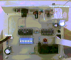
Initially, we used universal PCB to implement the receiver, transmitter and decoder, since wire-wrap wire not fixed on the PCB, resulted that the circuit operation quite unstable.
In order to eliminate the such problem, we made the PCB ourselves. At that time, we just route the traces as normal PCB design, the wire turned 90 degrees. Although, we got the better results than the initial one, but it still seems unstable, and we found the additional problems that the gain of op-amp is unsatisfied, the gain too small to amplify the signal received, Our project supervisor Mr. Poon suggested that the uA741 unstable for single voltage source configuration, should we change another one might carried out the satisfied results. Furthermore, the turns of antenna on receiver insufficient that significantly distorts the UHF signal transmitted from transmitting end.
From the study of the subject - Electronic Design Automation, we knew that the design methodology of high speed PCB significantly different from the normal (low frequency, i.e. frequency lower than 20MHz) PCB design, the 90 degrees turning point leads a major problem that just like an antenna to emit the high frequency, and the such frequency would interfered the surround circuit resulted in circuit unstable and eventually suspend the circuit. So, we change our PCB layout again that all turning point change to 45 degrees instead of the 90 degrees turning previously, and change also the op-amp from uA741 to MC4558 which supports a single positive voltage supplied.
At the final, this a auto dialer can not completely successful. We think that there are product many problem, as shown in the following ?
Firstly, we must know that the auto dialer sets like those used to dial a number or more calls, the receiver have be switchhook (on- or off-hook). We have know a information that as the follows points. It is simple in appearance and operation yet it performs a surprising number of functions. The most important ones are:
The principle of the how to detect busy tone that first we must know the central office how working ?
The central office must provide the ringing signal to the subscriber telephone to alert the called telephone that a call is waiting; therefore, the central office must apply the ringing signal to the line after the switching has completed the connection. This is done normally by a relay that is energized by the switch. The ringing signal is typically 90V rms. at 20Hz.
Detecting service requests (when the caller goes off-hook), the dialing input, and supervising calls in progress (when the ring is answered, or when either party hangs up) are accomplished by detecting the presence or absence of current flow in the loop. The requires a sensor that can discriminate accurately, regardless of line length, between off-hook current and current as a result of noise, leakage or a small standby current for the memory in an electronic dialer circuit. There are two common methods used for detecting a subscriber off-hook - loop start and ground start.
Loop start lines are used in the vast majority of local loop circuits; they signal off-hook by completing a circuit at the dialer. Figure C-16 illustrates a subscriber line interface using relays for sensing and logic. In the on-hook condition, neither the line relay nor the cut-off relay is operated, and the line relay battery provides power to the line. No current (except perhaps leakage current) flows because the switchhook contacts are open.
When the subscriber lifts the handset (Figure C-16a) current flows from the line battery through the closed switchhook contacts and energizes the line relay. A set of the line relay contacts close to signal the switching circuits, via the line finder, that the subscriber wishes service. When the line finder seizes the line to provide dial tone, it causes the cutoff relay to operate, which disconnects the line relay as shown in Figure C-16b, and extends the circuit into the switching equipment. This also disconnects the line battery so further operation is powered by another battery supply through the first selector or register of the switching system. Note that the line relay has two windings, one connected in each side of the line. The windings are balanced and wound so that voltages induced in the line are canceled; thus, only current that flows around the entire loop will cause the relay to operate.
Ground-start lines are used on loops connecting PBXs to the central office, and in other situations where it is desirable to detect a line that has been selected for use (seizure of the line) instantaneously from either end of the line. Grounding the ring-side path, as shown in Figure C-18, causes current to flow through one-half of the line relay which is sufficient to energize the relay. Further operation is as explained for loop start. When dial tone is detected by the PBX equipment, the ground-start contact is opened.
Appendix C Figure C-18 Ground-Start Signaling
The central office supplies the ringing signal. Service requests are detected by the presence or absence of current. A sensor monitors the line loop current, and detects significant changes. Two methods are used - loop start and ground start.
In loop start detection, a cutoff and line relays are used for sensing and logic. The line relay is energized when the switchhook contacts are closed. The line relay is disabled by the activation of the cutoff relay.
In ground start, the line relay may be activated by grounding the ring side of the line at any point. This configuration is usually used with PBX equipment.
Why choose ISD 1416P
Easy interface: The playback function can easily achieved by using either a falling edge or a low level.
This project carried out an unexpected problem. We are unfamiliar in telecommunication circuit design, so the auto dialer cannot meet the proposal we submitted. According to the proposal, the auto dialer be able to detect the busy tone / pickup and then dial another party. As the specification of IC MC145416 used, it is able to dial 3 different parties one by one as the previous number unsuccess to connect. The detailed episode during constructing auto dialer, please refer to discussion section.
There is an very important thing that the operating frequency may jam other government department infracommunication, such as police communication, so the Life-Saver must apply an approval before mass product to prevent that offend the law.
The Life-Saver we constructed adopt many future expansion functions for further purpose.
| Integrated an alarm system at the passage to inform neighbors there is an emergency. | |
| The 2262/2272 are able to support up to 6 channels, so Life-Saver can be used in elder care center. Each elder has one, then if there is an emergency, the nurse would knew who need the help. | |
| It also be a burglar alarm, if there is a crime, one can press to report to police. | |
| …… |
As the Life-Saver carried out dramatic features, functionality and flexibility, we have the confidence that it would got large market share and since we tried the best to reduce the cost (overall raw material cost only HKD137.64), resulted in lower retail price, it does not only strong the competitive but also provide benefit to elder.
This project not only help us engaged the theories from books and the practical design constrains, but also do a meaning thing to the society to help the senior citizens. Do not forget, we living in this prosperous land, because their hard working throughout the life yesterday!
Furthermore, we drafted a case for finished product, please see the appendix Z-1 and Z-2.
Understanding Telephone Electronics
3rd Edition
Stephen J. Bigelow
Motorola at
National Semiconductor Corp.
Information Storage Devices Corp.
It available on Internet at: